Z-Height Measurement
Z-height measurement, or any measurement of critical position in one axis, is a common need in many industries. Many engineers have struggled with trying to get an accurate measurement of sufficient resolution while coping with design requirements and implementation problems caused by limited space, temperature changes, vacuum, target surface interference, and damage to measurement probes resulting from incidental contact with the target.
Capacitive and eddy-current noncontact displacement sensors are becoming a standard technology for these applications because of their small size, flexibility, ease of use, high resolution, and robust design. Capacitive and eddy-current sensors can also be easily customized to fit in specific applications.
Recommended Equipment
Elite Series Capacitive Sensors
< 1 nm resolution, requires clean dry environment
Technologies
ECL202 Eddy-Current Sensor
< 100 nm resolution
Works in wet environment
Does not detect nonconductors
Many technologies have been applied to these z-height measurements, each with its own set of challenges. Contact gauging can damage target surfaces. Optical gauging can suffer from thermal sensitivity, inconsistent reflectivity of the target material, and may be difficult to fit in the space required. Some capacitive technologies can suffer damage to internal electronics if the end of the probe touches a grounded surface.
Lion Precision capacitive and eddy-current sensors are robust, thermally compensated, can have resolutions less than one nanometer, and bandwidths as high as 15 kHz. They can be used in vacuum and their low power dissipation will not add heat to your sensitive environment. They can also be customized for a perfect fit. Capacitive sensors provide the absolute highest resolution but must be used in a clean environment.
Eddy-Current sensors can be used in wet environments while still providing resolutions below 100 nm.Applications and Industries
Z-Height measurement is common in industries requiring precise positioning for optical and nonoptical processing. Some of the many applications include: semiconductor wafer processing and inspection, microlithography, optical and nonoptical microscopy, focus and prefocus, mask positioning and alignment, scanning control, and planarization.
These applications often require critical positioning where nanometers matter. They also can include challenging environments from slurry filled environments of chemical-mechanical planarization to the vacuum environments requiring low outgassing and low power dissipation.
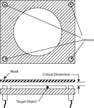
Mask Alignment
Masks used in semiconductor processing must be precisely aligned to achieve today's circuit densities. Four noncontact probes can be mounted to monitor z-height and parallelism of the mask relative to the wafer. Maintaining equal outputs from the sensors provides parallelism while the actual output value indicates the critical gap dimension.
Chemical-Mechanical Planarization
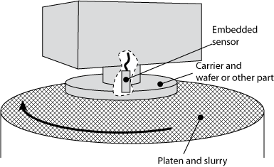
A precise lapping process is used in semiconductor, disk drive, and other industries that require accurately controlled depth of material removal. The chemical-mechanical planarization process uses an abrasive slurry on a precision platen that turns against the object to be lapped. As material is removed, the carrier holding the object being lapped moves closer to the platen. Eddy-current sensors do not detect the slurry and thereby provide a precise measurement of the relative position of the platen to the carrier (z-height) to determine how much material has been removed. High resolution of the sensors enable measurements to within 100 nm. For semiconductor wafers, the eddy-current sensors can "see through" the wafer and the slurry to measure the distance to the platen.
Focus/Prefocus
Optical and nonoptical microscopy require precise z-height positioning to maintain proper focus. While optical algorithms exist for controlling focus, they can be slow while searching for the correct focus. Noncontact sensors can be used to quickly move to a position very near the precise focal length where the optical algorithms can more quickly complete the process.
Because of limited space and extreme demand for performance in many microscopy applications, there are significant advantages to using custom designed probes; this drawing shows capacitive probes configured at 45°.
Scanning
Some processing and inspection applications use a scanning head to treat or inspect across the surface of the target object. Z-height gap and alignment are still critical, but rather than a static control, this application is dynamic. Lion Precision capacitive and eddy-current sensors have wide bandwidths of 15 kHz with bandwidths as high as 80 kHz when required. The fast response time and excellent phase response enable precise and stable servo control in dynamic applications.
Article published with the agreement of Copyright © 2011 Lion Precision.

Home - Search - Suppliers - Links - New Products - Catalogues - Magazines
Problem Page - Applications - How they work - Tech Tips - Training - Events -